Electronics is the branch of science that deals with the study and control of the flow of electrons in devices and circuits. This chapter covers semiconductors (N-type and P-type), the PN junction and how a semiconductor diode allows current to flow in only one direction, and the light-emitting diode (LED), which emits light when electrons recombine with holes.
It also compares analog and digital electronics, explains how an analog-to-digital converter (ADC) samples, quantizes, and encodes signals, introduces Boolean logic and the bit/byte, and covers the five basic logic gates (AND, OR, NOT, NAND, NOR) with their circuit symbols, logic equations, and truth tables, closing with real-world applications in burglar alarms and fire alarm systems.
Learning Objectives
- Describe the working of a semiconductor diode, including forward and reverse bias and the depletion region
- Describe the action of a light-emitting diode (LED) in passing current in one direction and emitting light
- Compare analog and digital electronics, and describe the role of an analog-to-digital converter (ADC)
- Explain that electronic devices are built from digital logic circuits that convert incoming voltage into binary pulses (1 or 0)
- Explain that Boolean logic is the basis for converting analog data to digital data, and define 'bit' and 'byte'
- State in words and in truth table form the action of AND, OR, NAND, NOR, and NOT logic gates
- Use standard circuit symbols for logic gates, and write their logic equations
- Identify the use of logic gates for security purposes, such as burglar alarms and fire alarm systems
- Determine, for given problems, how combinations of Boolean switches achieve logical operations
Key Concepts
19.1 Semiconductors
Semiconductors are materials whose electrical conductivity lies between that of conductors and insulators; the most common semiconductors are silicon (Si) and germanium (Ge), and their conductivity can be increased by adding a small amount of impurity — a process called doping. In an N-type semiconductor, a small amount of a pentavalent impurity (such as phosphorus or arsenic, with five valence electrons) is added to silicon: four of its electrons form covalent bonds with silicon atoms, while the fifth remains free to move, and these free electrons become the majority charge carriers, increasing conductivity.
In a P-type semiconductor, a trivalent impurity (such as boron or gallium, with three valence electrons) is added to silicon instead; since one bond remains incomplete, this creates a hole (a missing electron), and holes act as positive charge carriers that move through the crystal, helping conduct current.
19.2 PN Junction and the Semiconductor Diode
When N-type and P-type semiconductors are joined together, they form a PN junction (semiconductor diode). At the junction, electrons from the N-side and holes from the P-side recombine, creating a depletion region — a zone without free charge carriers that acts as a barrier preventing further charge movement. An external voltage must be applied to overcome this barrier before current can flow: about 0.7 V for silicon diodes, and about 0.3 V for germanium diodes.
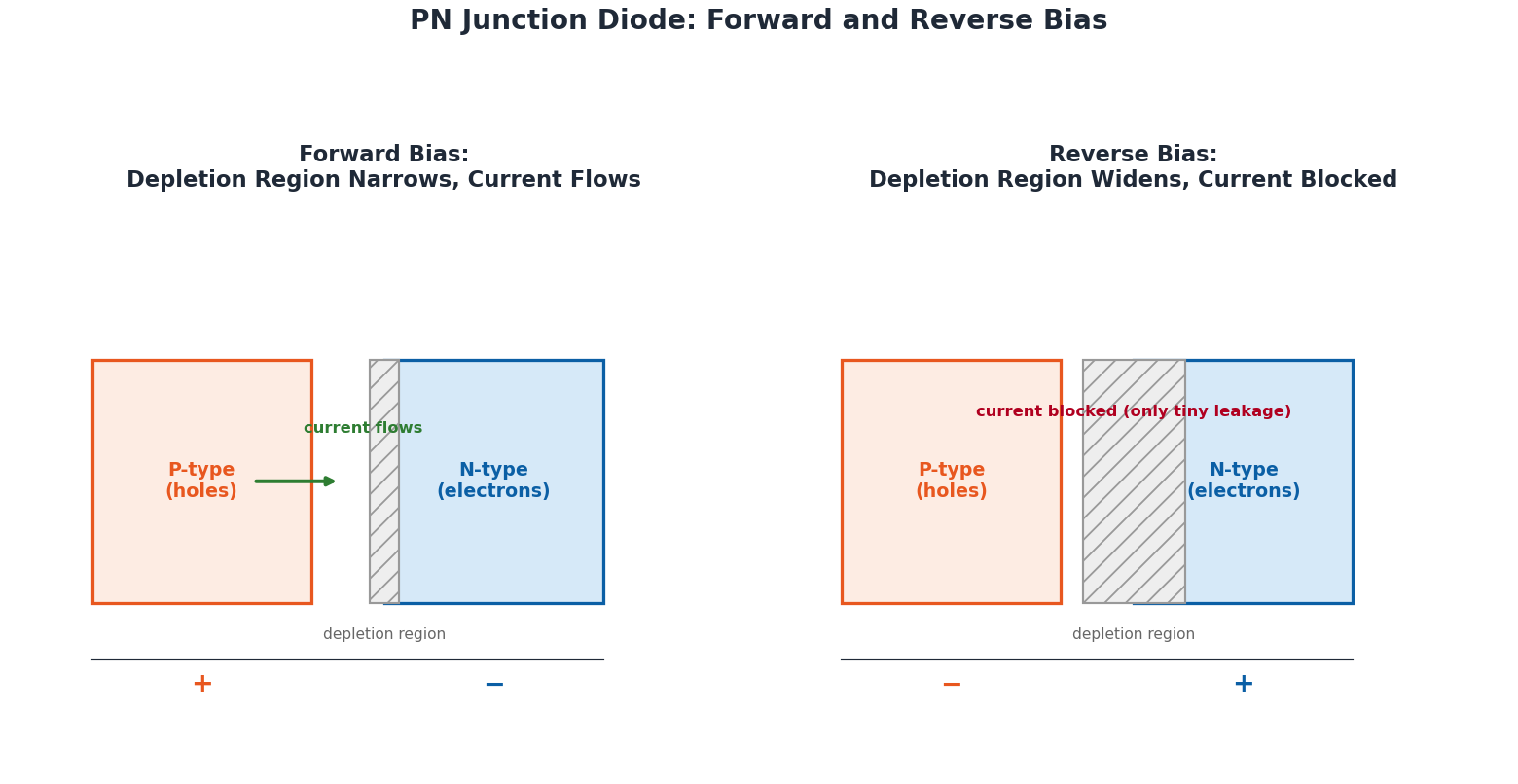
A semiconductor diode allows current to flow in only one direction. When the P-side is connected to the positive terminal and the N-side to the negative terminal of a battery, the diode is forward biased: the applied voltage reduces the potential barrier and narrows the depletion region, letting charge carriers cross easily and current flow. When the P-side is connected to the negative terminal and the N-side to the positive terminal, the diode is reverse biased: the depletion region widens, the potential barrier increases, and the flow of majority carriers is blocked — though a very small leakage current still flows due to minority carriers. The diode's current-voltage (I-V) characteristic curve shows significant current only in forward bias, with the current almost completely blocked in reverse bias — a property essential to rectifiers, voltage regulators, and electronic switches.
19.3 Light-Emitting Diode (LED)
A Light-Emitting Diode (LED) is a semiconductor device built from a PN junction that, like a regular diode, allows current to flow in only one direction, but additionally emits light when electrons recombine with holes. When forward biased, the applied voltage reduces the depletion region, allowing charge carriers to flow across the junction; as electrons from the N-type material cross over and recombine with holes in the P-type material, energy is released in the form of photons, producing visible light.
In reverse bias, the depletion region widens, blocking current flow, so no light is emitted — LEDs are therefore designed to function only under forward bias. On the LED's I-V characteristic graph, only a small current flows initially as voltage increases, but beyond a threshold voltage, current increases sharply and light emission begins. The colour of light emitted depends on the semiconductor materials used in manufacturing, which affect the wavelength of the emitted photons. LEDs are efficient, durable, and energy-saving, converting electrical energy directly into light (unlike filament bulbs, which waste much energy as heat) and are used in radios, lamps, digital clocks, calculators, video displays, remote controls, and modern lighting.
19.4 Analog and Digital Electronics
Electronic circuits are broadly divided into analog and digital types. In analog circuits, voltages and currents vary smoothly and continuously within a range (e.g., an analog meter's pointer moving over a continuous scale) — used in devices like amplifiers and dimmer switches that need a wide range of adjustment. In digital circuits, voltages have only two possible values — 'high' (e.g., 5 V) or 'low' (e.g., near 0 V) — used in switching systems such as a simple ON/OFF lamp switch; digital electronics now extend well beyond computers into telephones, radar systems, industrial machines, and household appliances.
Since everyday quantities like sound and light are analog and cannot be processed directly by digital circuits, an analog-to-digital converter (ADC) is used to convert analog signals into digital binary form; the ADC works by sampling the analog signal at regular intervals and converting each sample into a binary number representing its voltage level.
19.5 Conversion from Analog to Digital Data
Analog data (such as sound or light) is continuous and can take any value within a range, while digital systems use discrete binary data (0s and 1s). Converting analog data into digital form involves three steps: (1) Sampling — the continuous analog signal is measured at regular intervals; (2) Quantization — each sampled value is rounded to the nearest predefined level; (3) Encoding — the quantized values are converted into binary numbers. For example, a sound wave is sampled at regular intervals, each value quantized, and then encoded into binary, making the sound usable by digital devices; a digital-to-analog converter (DAC) later reverses this process, converting binary data back into an analog signal for output — such as playing sound through a speaker.
19.6 Boolean Logic
A binary variable has only two possible states, like a switch that is either ON (closed, represented as 1) or OFF (open, represented as 0). In a simple circuit with a battery, lamp, and switch, when the switch is open (input = 0), no current flows and the lamp is OFF (output = 0); when the switch is closed (input = 1), the lamp turns ON (output = 1). George Boole developed Boolean algebra — the foundation of digital electronics and computing — using binary values called bits, where each bit is either 0 or 1; eight bits together form a byte, the basic unit used to represent data in computers.
Boolean algebra is used in the ADC, which converts continuous analog data into discrete digital data, and forms the basis for designing all digital systems. It defines three basic logic operations — AND, OR, and NOT — implemented physically using logic gates: digital circuits with binary inputs and a binary output. In an AND-gate circuit, a lamp connected in series with two switches S1 and S2 only lights when both switches are closed (both inputs = 1); in an OR-gate circuit, switches S1 and S2 are placed in parallel, so the lamp lights if either or both switches are closed (at least one input = 1).
19.7 Logic Gates
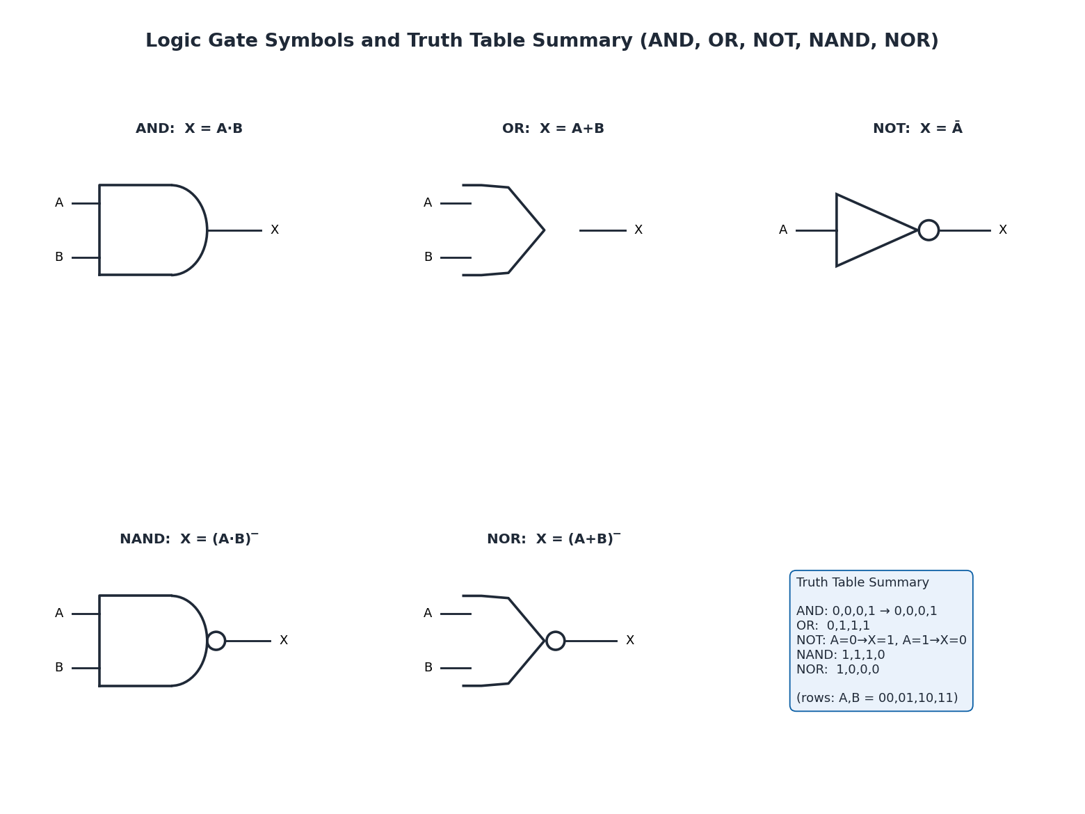
A logic gate is a basic digital circuit component that performs a logical operation; most logic gates have two inputs and one output, except the NOT gate, which has a single input and single output. The AND gate's output X is 1 only if both inputs A and B are 1, written as X = A·B. The OR gate's output is 0 only if both inputs are 0 (otherwise 1), written as X = A+B. The NOT gate (or inverter) has one input and inverts it — if the input is 1, the output is 0, and vice versa — written as X = Ā.
A NAND gate is an AND gate combined with a NOT gate (an AND gate symbol with a bubble at its output); its logic equation is X = (A·B)‾, and its output is 0 only when both A and B are 1, otherwise 1. A NOR gate is an OR gate combined with a NOT gate (an OR gate symbol with a bubble at its output); its logic equation is X = (A+B)‾, and its output is 1 only when both A and B are 0, otherwise 0. These simple gates can be combined to build the complex digital systems found in computers and smartphones.
19.8 Applications of Logic Gates
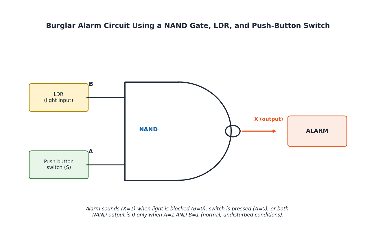
A simple burglar alarm can be built using a single NAND gate, a light-dependent resistor (LDR), a push-button switch (S), and an alarm. The LDR connects to one NAND input (B) and the battery's positive terminal, while the switch (S) connects to the other input (A), with the alarm connected to the output. Normally, light on the LDR keeps its resistance low, keeping input B high (1); if a burglar blocks the light, the LDR's resistance rises, making B low (0). Similarly, stepping on the switch makes input A low (0). Since a NAND gate outputs low (0) only when both inputs are high (1), the alarm — which is triggered by a high (1) output — will sound if the light is blocked, the switch is pressed, or both, effectively detecting unauthorized entry.
A fire alarm system detects fire early by sensing smoke and heat, triggering an alarm to warn people in time to act; it consists of alarm-starting devices (smoke detectors, heat sensors), alarm devices (sirens), fire control systems (sprinklers), and power supplies. While advanced, expensive systems exist, a basic fire alarm can be built using simple components (thermistors, an operational amplifier, germanium diodes, a voltage regulator, and a timer IC), or using basic logic gates that process inputs from smoke and heat sensors and trigger the alarm when either condition (smoke OR heat) is met — an affordable, efficient fire detection solution using an OR-gate-based design.
Important Definitions
Define a semiconductor.
A material whose electrical conductivity lies between that of a conductor and an insulator; common examples are silicon and germanium, whose conductivity can be increased by doping.
What is doping?
The process of adding a small amount of impurity to a semiconductor to increase its electrical conductivity, producing N-type (pentavalent impurity) or P-type (trivalent impurity) material.
Define a PN junction.
The boundary formed when N-type and P-type semiconductors are joined together, creating a depletion region that acts as a semiconductor diode, allowing current to flow in only one direction.
What is forward bias?
The condition where the P-side of a diode is connected to the positive terminal and the N-side to the negative terminal of a battery, narrowing the depletion region and allowing current to flow easily.
What is a light-emitting diode (LED)?
A PN-junction semiconductor device that allows current to flow in one direction and emits light (photons) when electrons recombine with holes under forward bias.
Define a bit and a byte.
A bit is the smallest unit of data in computing, either 1 or 0; a byte is a group of eight bits, used as a basic unit for representing data in computers.
What is a logic gate?
A basic digital circuit with binary inputs and a binary output that performs a specific logical operation (such as AND, OR, or NOT), forming the building blocks of digital electronics.
What is an analog-to-digital converter (ADC)?
A device that converts a continuous analog signal into discrete digital binary data by sampling the signal at regular intervals, quantizing each sample, and encoding it into binary.
Key Formulas
| Topic | Formula |
|---|---|
| AND gate logic equation | X = A · B |
| OR gate logic equation | X = A + B |
| NOT gate logic equation | X = Ā (NOT A) |
| NAND gate logic equation | X = (A · B)‾ (NOT of A AND B) |
| NOR gate logic equation | X = (A + B)‾ (NOT of A OR B) |
| Silicon diode forward voltage (approx.) | ≈ 0.7 V |
| Germanium diode forward voltage (approx.) | ≈ 0.3 V |
| Byte definition | 1 byte = 8 bits |
Diagrams
PN Junction Diode: Forward and Reverse Bias: A PN junction diode showing the narrowed depletion region and current flow in forward bias, compared with the widened depletion region blocking current in reverse bias
Logic Gate Symbols and Truth Tables: Circuit symbols and truth tables for the five basic logic gates: AND, OR, NOT, NAND, and NOR
Burglar Alarm Circuit Using a NAND Gate: A NAND-gate burglar alarm circuit with an LDR (light input) and a push-button switch as its two inputs, triggering the alarm output when light is blocked or the switch is pressed
Short Questions & Answers
What is the function of a semiconductor diode?
A semiconductor diode allows electric current to flow in only one direction (forward bias) while blocking it in the opposite direction (reverse bias), making it useful in rectifiers and switches.
What happens when a diode is forward biased?
The applied voltage reduces the potential barrier and narrows the depletion region at the PN junction, allowing charge carriers to cross easily and current to flow through the diode.
Why does an LED emit light when current passes through it?
In forward bias, electrons from the N-type material cross the junction and recombine with holes in the P-type material; this recombination releases energy in the form of photons, producing visible light.
What does an analog-to-digital converter (ADC) do?
An ADC converts a continuous analog signal into discrete digital binary data by sampling the signal at regular intervals, quantizing each sample to the nearest level, and encoding it into binary numbers.
What is the difference between analog and digital signals?
Analog signals vary smoothly and continuously over a range of values, like a sound wave; digital signals have only two discrete values, 'high' (1) and 'low' (0), like a series of ON/OFF pulses.
What is Boolean logic in digital electronics?
Boolean logic (developed by George Boole) is a system of algebra using binary values (0 and 1, or bits) to represent and process logical operations such as AND, OR, and NOT — the foundation of digital circuits and computing.
What does a NOT gate do in a digital circuit?
A NOT gate (inverter) has a single input and inverts it: if the input is 1, the output is 0, and if the input is 0, the output is 1.
What is the role of an AND gate in digital circuits?
An AND gate produces an output of 1 only when all of its inputs are 1; if any input is 0, the output is 0 — modelled by switches connected in series, where the lamp lights only if all switches are closed.
Long Questions & Answers
Explain how the depletion region of a PN junction diode changes under forward and reverse bias, and describe the effect this has on current flow.
A PN junction is formed when N-type and P-type semiconductor materials are joined together; at the junction, free electrons from the N-side and holes from the P-side recombine, forming a narrow region depleted of free charge carriers, called the depletion region, which acts as a natural barrier resisting further charge movement across the junction. When the diode is connected in forward bias — with the P-side joined to the positive terminal of a battery and the N-side to the negative terminal — the applied external electric field opposes and reduces this internal barrier: it pushes the remaining free electrons in the N-region and holes in the P-region back toward the junction, narrowing the depletion region and effectively lowering the potential barrier that charge carriers must overcome. Once the applied voltage exceeds a certain threshold (about 0.7 V for silicon or 0.3 V for germanium), the depletion region becomes narrow enough that electrons and holes can cross the junction freely and recombine continuously, allowing a substantial current to flow through the diode as long as the forward voltage is maintained. In contrast, when the diode is connected in reverse bias — with the P-side joined to the negative terminal and the N-side to the positive terminal — the applied field pulls the free electrons in the N-region and holes in the P-region further away from the junction, widening the depletion region and increasing the height of the potential barrier; because there are now even fewer available charge carriers immediately at the junction and the barrier is stronger, the flow of majority charge carriers is almost completely blocked, and only a very small leakage current continues to flow, carried by minority charge carriers (thermally generated electrons and holes) present on each side of the junction. This asymmetric behaviour — free current flow in forward bias, and almost complete blocking in reverse bias — is precisely what makes the diode useful as a one-way valve for electric current, and underlies its applications in rectifier circuits (converting AC to DC), voltage regulators, and simple electronic switches.
Describe how a light-emitting diode (LED) produces light, and explain how the semiconductor material used affects the colour of light emitted.
A light-emitting diode (LED) is a specially constructed PN-junction semiconductor device that, like an ordinary diode, permits current to flow in only one direction, but which additionally converts a portion of the electrical energy passing through it directly into light. When an LED is connected in forward bias, the applied voltage reduces the width of the depletion region at the PN junction in the same way as in an ordinary diode, allowing free electrons from the N-type material and holes from the P-type material to cross the junction and meet in large numbers. As each electron crosses into the P-type region and recombines with a hole, it drops from a higher-energy state (in the conduction band) to a lower-energy state (in the valence band), and the specific amount of energy released in this transition is emitted as a single discrete packet of electromagnetic energy — a photon of light — rather than being dissipated primarily as heat, as happens in an ordinary diode or resistor. This is why LEDs are far more energy-efficient than traditional filament bulbs, which waste much of their input energy as heat rather than useful light. The particular colour (wavelength) of light produced by a given LED depends directly on the size of the energy gap between the conduction band and valence band of the specific semiconductor compound used in its manufacture — different combinations of semiconductor materials (rather than just silicon alone, as in ordinary diodes, LEDs are often made from compound semiconductors such as gallium arsenide phosphide or gallium nitride, chosen and engineered to produce specific energy gaps) release photons of correspondingly different energies when electrons recombine with holes, and since a photon's energy directly determines its wavelength (and hence its perceived colour), manufacturers can produce LEDs that emit red, green, blue, or other specific colours of light simply by choosing the appropriate semiconductor material and, in some cases, adding further impurities to fine-tune the exact energy gap and resulting colour.
What is Boolean logic, and how do logic gates use it to process binary data? Illustrate your answer with the logic equations and truth tables of the AND, OR, and NOT gates.
Boolean logic, developed by the mathematician George Boole, is a formal system of algebra that operates exclusively on binary variables — quantities that can take only one of two possible values, conventionally represented as 1 (true, high, or ON) and 0 (false, low, or OFF). This binary framework maps naturally onto simple electrical circuits: for instance, in a circuit containing a battery, a switch, and a lamp, the state of the switch (open or closed) can be treated as a binary input (0 or 1), and the resulting state of the lamp (OFF or ON) as a binary output, following logical rules that depend on how the circuit is wired. This binary system — where the smallest unit of data, called a bit, is either 0 or 1, and a group of eight bits forms a byte — underlies all of modern digital electronics and computing, and is also what makes possible devices like the analog-to-digital converter (ADC), which uses Boolean-based binary encoding to represent continuously varying real-world analog signals (like sound or light) as sequences of discrete digital values that computers can process. Boolean algebra defines a small set of fundamental logical operations, which are physically implemented in electronic circuits called logic gates — devices with one or more binary inputs and a single binary output, whose output value depends entirely on the specific combination of input values according to a fixed logical rule. The AND gate, with two inputs A and B, produces an output X that is 1 only when both A AND B are simultaneously 1 (X = A·B); its truth table shows an output of 0 for every input combination except A=1, B=1, matching the behaviour of two switches wired in series, where a lamp lights only when both switches are closed. The OR gate, similarly with two inputs A and B, produces an output X that is 1 if either A OR B (or both) is 1, and 0 only when both inputs are 0 (X = A+B); its truth table matches two switches wired in parallel, where the lamp lights if at least one switch is closed. The NOT gate, unlike the other two, has only a single input A and simply inverts it, producing an output X that is the opposite of A (X = Ā) — if A is 1, X is 0, and if A is 0, X is 1; because of this inverting behaviour, the NOT gate is also commonly called an inverter. By combining these three fundamental gates — and derived gates such as NAND and NOR, which add an inverter to the output of an AND or OR gate respectively — engineers can construct arbitrarily complex digital logic circuits, from simple alarm systems to the processors found in modern computers and smartphones, all built up systematically from these basic binary building blocks.
Explain how a burglar alarm can be designed using a single NAND gate and a light-dependent resistor (LDR), describing how the circuit responds to different scenarios of unauthorized entry.
A practical and inexpensive burglar alarm circuit can be built using just a single NAND gate together with a light-dependent resistor (LDR), a push-button switch (S), a suitable power supply, and an alarm device connected to the gate's output. In this design, the LDR is connected to one input of the NAND gate, labelled B, in such a way that when ordinary ambient light falls on the LDR, its electrical resistance is low, which results in input B receiving a high logic level (B = 1); the push-button switch S is connected to the NAND gate's other input, labelled A, wired so that under normal, undisturbed conditions (switch not pressed) input A also remains at a high logic level (A = 1). Recalling that a two-input NAND gate produces a low output (0) only in the single case where both of its inputs are simultaneously high (1), and produces a high output (1) in every other combination of inputs, this circuit is deliberately designed so that during normal conditions — full light falling on the LDR (B=1) and the switch not pressed (A=1) — both inputs to the NAND gate are high, and so the NAND gate's output remains low (0), meaning the alarm (which is designed to sound only on a high, 1, output signal) stays silent. However, if a burglar attempting to enter blocks the light falling on the LDR (for example, by physically covering a light sensor placed at an entry point, or by their body blocking a light beam aimed at the LDR), the LDR's resistance rises sharply, causing input B to switch to a low logic level (B=0); alternatively, if the burglar steps on or otherwise triggers the push-button switch S (which might be concealed under a doormat or floor panel at the entry point), input A switches to a low logic level (A=0). In either of these two disturbance scenarios — B=0 with A=1, or A=0 with B=1 — or even in the case where both inputs simultaneously become 0 (both the light is blocked and the switch is triggered together), the crucial condition for a low NAND output (both inputs high) is no longer satisfied, so the NAND gate's output switches to high (1), which immediately activates and sounds the connected alarm. In this way, a single NAND gate, exploiting its particular truth table behaviour, elegantly and reliably provides burglar-detection coverage against two independent types of intrusion (light interruption and physical pressure) using just one simple logic gate.
Multiple Choice Questions (MCQs)
A diode allows current to flow in: (A) both directions (B) neither direction (C) one direction only (D) random directions
Correct answer: (C) one direction only. A semiconductor diode is designed to allow current to flow in only one direction (forward bias) and block it in the reverse direction.
What is the primary function of a light-emitting diode? (A) To block current in both directions (B) To emit light when current passes in one direction (C) To amplify electrical signals (D) To convert light into electrical energy
Correct answer: (B) To emit light when current passes in one direction. An LED emits light as electrons recombine with holes at the PN junction when current flows through it in forward bias.
The output of a two-input NOR gate is '1' when: (A) A is '1' and B is '0' (B) A is '0' and B is '1' (C) both A and B are '0' (D) both A and B are '1'
Correct answer: (C) both A and B are '0'. A NOR gate's output is 1 only when both inputs are 0; otherwise, the output is 0.
The output of a NAND gate is '0', when: (A) both of its inputs are '0' (B) both of its inputs are '1' (C) any of its inputs is '0' (D) any of its inputs is '1'
Correct answer: (B) both of its inputs are '1'. A NAND gate's output is 0 only when both inputs are 1; for any other input combination, the output is 1.
How many bits make up a byte in Boolean logic? (A) 2 (B) 4 (C) 6 (D) 8
Correct answer: (D) 8. A byte is formed from eight bits, and represents a basic unit of data in computing.
The logic equation for an AND gate is written as: (A) X = A + B (B) X = Ā (C) X = A · B (D) X = (A·B)‾
Correct answer: (C) X = A · B. The AND gate's logic equation is X = A · B, meaning the output X is 1 only if both inputs A and B are 1.
A semiconductor diode is forward biased when: (A) the P-side is connected to the negative terminal (B) the N-side is connected to the negative terminal (C) both terminals are left unconnected (D) the P-side and N-side are both connected to the positive terminal
Correct answer: (B) the N-side is connected to the negative terminal. In forward bias, the P-side connects to the positive terminal and the N-side to the negative terminal, narrowing the depletion region and allowing current to flow.
An analog-to-digital converter (ADC) works by: (A) amplifying the analog signal only (B) sampling, quantizing, and encoding the analog signal into binary (C) converting binary data back into an analog signal (D) blocking all analog signals
Correct answer: (B) sampling, quantizing, and encoding the analog signal into binary. An ADC converts analog signals to digital form through three steps: sampling at regular intervals, quantizing to the nearest level, and encoding into binary numbers.
In an N-type semiconductor, the majority charge carriers are: (A) holes (B) free electrons (C) protons (D) neutrons
Correct answer: (B) free electrons. N-type semiconductors are doped with a pentavalent impurity, providing extra free electrons as the majority charge carriers.
A basic burglar alarm can be built using a NAND gate together with: (A) a transformer and a diode (B) an LDR and a push-button switch (C) a CRO and an ammeter (D) a step-up transformer and a relay
Correct answer: (B) an LDR and a push-button switch. A NAND gate combined with an LDR (light input) and a push-button switch (pressure input) can trigger an alarm when light is blocked or the switch is pressed.
Quick Revision Summary
- Semiconductors: N-type (pentavalent doping, free electrons = majority carriers), P-type (trivalent doping, holes = majority carriers)
- PN junction = diode; depletion region narrows in forward bias (current flows), widens in reverse bias (current blocked, small leakage only)
- Forward voltage: ≈0.7 V (silicon), ≈0.3 V (germanium)
- LED: forward-biased PN junction; electron-hole recombination releases photons (light); colour depends on semiconductor material
- Analog: continuous values; Digital: only 'high' (1) / 'low' (0); ADC = sampling → quantization → encoding
- Bit = smallest data unit (0 or 1); Byte = 8 bits
- AND: X=A·B (output 1 only if all inputs 1); OR: X=A+B (output 1 if any input 1); NOT: X=Ā (inverts input)
- NAND: X=(A·B)‾ (output 0 only if both inputs 1); NOR: X=(A+B)‾ (output 1 only if both inputs 0)
- Burglar alarm: NAND gate + LDR + switch — alarm sounds when light blocked OR switch pressed (output goes high)
- Fire alarm: smoke/heat sensors + logic gates (typically OR-based) trigger alarm when either condition is met
Exam Tips
- Always state BOTH the logic equation and the truth table when answering logic gate questions — many exams award marks for each separately
- Remember the two exceptions: NOT gate has only ONE input (all other gates covered here have two), and NAND/NOR gates are simply AND/OR gates with an inverted (bubbled) output
- For diode bias questions, remember: forward bias narrows the depletion region (current flows); reverse bias widens it (current blocked)
- Memorize the approximate forward voltages: silicon ≈ 0.7 V, germanium ≈ 0.3 V — commonly tested as direct recall questions
- For ADC questions, always list all three steps in order: sampling → quantization → encoding
- For burglar/fire alarm questions, explain the physical scenario (light blocked, switch pressed, smoke/heat detected) AND link it explicitly to the gate's truth table output that triggers the alarm