This chapter covers Electronics from the 2nd Year (FSc Part-II) Physics syllabus of the Punjab Curriculum and Textbook Board (PTB/PCTB). It studies the p-n junction and its use in rectification, special diodes, the transistor as an amplifier and switch, the operational amplifier, digital systems and logic gates. These notes are prepared by freebooks.pk.
Electronics is built on semiconductor devices such as diodes and transistors. This chapter explains how these small components rectify current, amplify signals, switch circuits and carry out logic, forming the basis of every electronic device.
Learning Objectives
- Describe the p-n junction and its forward and reverse characteristics.
- Explain rectification using diodes.
- Describe specially designed diodes such as the LED and photodiode.
- Explain the transistor as an amplifier and as a switch.
- Describe the operational amplifier and its uses.
- Explain digital systems and the fundamental logic gates.
Key Concepts
The p-n Junction
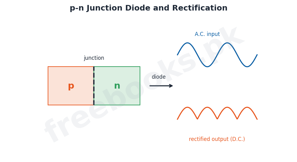
A p-n junction is formed when a p-type semiconductor (with positive charge carriers called holes) is joined to an n-type semiconductor (with free electrons). At the junction electrons and holes combine, leaving a thin depletion region with a potential barrier. When the junction is forward biased (p connected to + and n to -) the barrier is lowered and a current flows easily; when it is reverse biased the barrier is raised and almost no current flows. A p-n junction therefore conducts in only one direction and acts as a diode.
Rectification
Rectification is the process of converting alternating current into direct current, and it makes use of the one-way conduction of a diode. In half-wave rectification a single diode allows only one half of each A.C. cycle to pass, giving a pulsating one-directional output. In full-wave rectification an arrangement of diodes (such as a bridge of four diodes) uses both halves of the cycle, giving a smoother, more efficient direct output. Rectifiers are used in the power supplies of nearly all electronic equipment.
Specially Designed Diodes
Some p-n junctions are designed for special purposes. A light-emitting diode (LED) gives out light when it is forward biased and is used in displays and indicators. A photodiode does the reverse: it conducts more when light falls on it, and is used to detect light. A photovoltaic (solar) cell converts light energy directly into electrical energy. These devices show the close link between electricity and light in semiconductors.
The Transistor
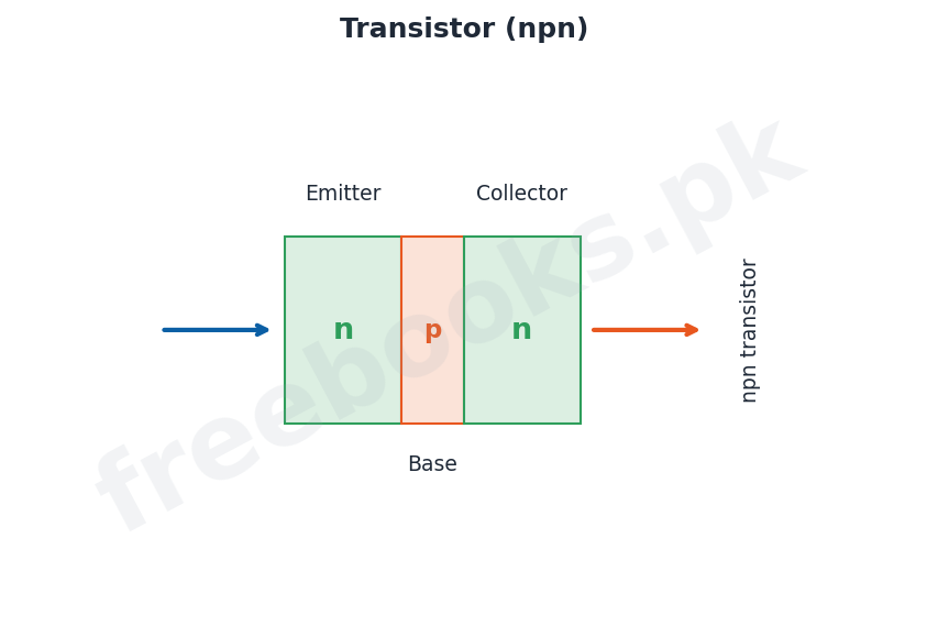
A transistor is a semiconductor device with three regions, either n-p-n or p-n-p, called the emitter, base and collector. A small current fed into the base controls a much larger current flowing between the collector and emitter. This ability of a small signal to control a large one makes the transistor the key active component of modern electronics.
Transistor as an Amplifier and Switch
Because a small base current controls a large collector current, a transistor can be used as an amplifier: a weak input signal applied to the base produces a much stronger copy of it in the collector circuit, as in radios and audio systems. A transistor can also be used as a switch: a small base voltage can turn the large collector current fully on or completely off, so the transistor acts like an electrically controlled switch, which is the basis of digital circuits.
The Operational Amplifier
The operational amplifier (op-amp) is a high-gain amplifier with two inputs, an inverting input and a non-inverting input, and one output; it amplifies the difference between the two inputs. With suitable external resistors it can be connected as an inverting amplifier (output inverted and scaled), a non-inverting amplifier (output in phase and scaled) or a comparator (which compares two voltages and switches its output high or low according to which is larger). Op-amps are versatile building blocks used throughout analogue electronics.
Digital Systems and Logic Gates
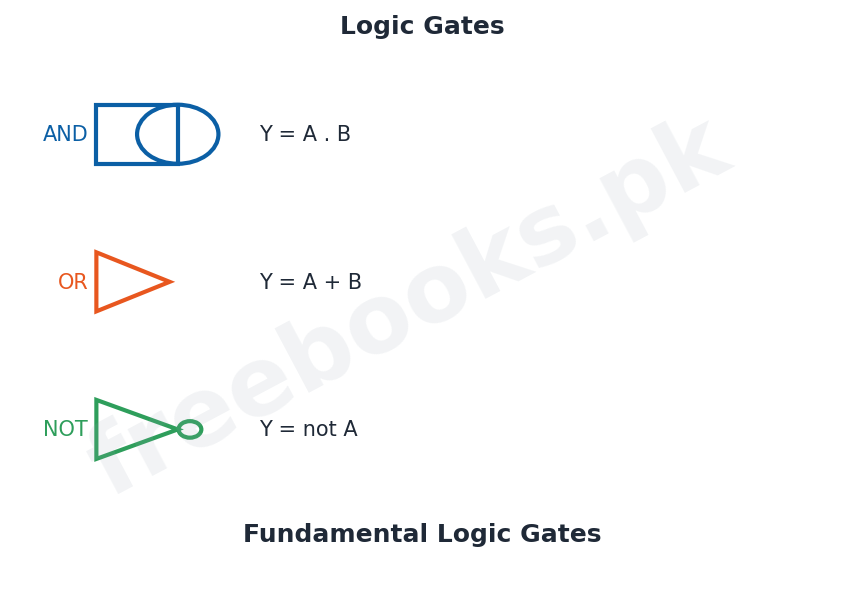
In a digital system information is handled using just two states, usually written 1 (high) and 0 (low), rather than a continuously varying signal. The basic building blocks that process these binary signals are logic gates. The three fundamental gates are the AND gate (output 1 only when all inputs are 1, Y = A.B), the OR gate (output 1 when any input is 1, Y = A + B) and the NOT gate or inverter (output the opposite of the input). Combining these gives all the logic needed for computers and digital devices.
Other Logic Gates
From the fundamental gates other useful gates are built. The NAND gate is an AND gate followed by a NOT, and the NOR gate is an OR gate followed by a NOT; these two are called universal gates because any logic function can be made from them alone. The XOR (exclusive-OR) gate gives an output of 1 only when its two inputs are different. Networks of such gates are used in control systems, for example to switch a device on automatically when certain conditions are met.
Important Definitions
p-n junction
The boundary formed when p-type and n-type semiconductors are joined; acts as a diode.
Forward bias
Connecting a diode so that it conducts (p to +, n to -).
Rectification
The conversion of alternating current into direct current using diodes.
LED
A diode that emits light when forward biased.
Transistor
A three-region semiconductor device in which a small base current controls a large current.
Operational amplifier
A high-gain amplifier that amplifies the difference between its two inputs.
Logic gate
A circuit that processes binary (1/0) signals.
Universal gate
A gate (NAND or NOR) from which any logic function can be made.
Formulas & Rules
| Item | Fact |
|---|---|
| AND gate | Y = A . B |
| OR gate | Y = A + B |
| NOT gate | Y = complement of A |
| NAND gate | Y = complement of (A . B) |
| NOR gate | Y = complement of (A + B) |
Diagrams & Illustrations
p-n junction diode: a p-n junction diode with p and n regions and the junction, converting an alternating input into a rectified one-directional output.
Transistor: an n-p-n transistor showing the emitter, base and collector regions, where a small base current controls a large collector current.
Logic gates: the symbols of the three fundamental logic gates: AND (Y = A.B), OR (Y = A + B) and NOT (inverter).
Solved Examples & Numericals
Diode conduction
A diode conducts when forward biased (p to +, n to -) and blocks when reverse biased, so it passes current in only one direction.
Half-wave rectifier
In half-wave rectification a single diode passes only one half of each A.C. cycle, giving a pulsating direct output.
AND gate
For an AND gate with inputs A = 1 and B = 0, the output is Y = A.B = 1.0 = 0.
OR gate
For an OR gate with inputs A = 1 and B = 0, the output is Y = A + B = 1 + 0 = 1.
Short Questions & Answers
What is a p-n junction?
The boundary formed when p-type and n-type semiconductors are joined; it conducts in only one direction and acts as a diode.
What is rectification?
The conversion of alternating current into direct current using the one-way conduction of a diode.
What is an LED?
A light-emitting diode, which gives out light when it is forward biased.
How does a transistor amplify?
A small base current controls a much larger collector current, so a weak input signal produces a stronger output.
What is an operational amplifier?
A high-gain amplifier that amplifies the difference between its inverting and non-inverting inputs.
Why are NAND and NOR called universal gates?
Because any logic function can be built using only NAND gates or only NOR gates.
Long Questions & Answers
Q1: Describe the p-n junction and explain how it is used for rectification.
A p-n junction is formed by joining a piece of p-type semiconductor, in which the majority charge carriers are positive holes, to a piece of n-type semiconductor, in which the majority carriers are free electrons. Where they meet, electrons from the n-side and holes from the p-side combine, leaving behind a thin region free of mobile carriers called the depletion region, across which a small potential barrier is set up. The behaviour of the junction depends on how it is connected to a battery. When it is forward biased, with the p-side joined to the positive terminal and the n-side to the negative, the applied voltage lowers the barrier and a current flows easily across the junction. When it is reverse biased, the barrier is raised and only an extremely small current flows. A p-n junction therefore allows current to pass in one direction only and is called a diode. This one-way property is used for rectification, the process of turning alternating current into direct current. In a half-wave rectifier a single diode conducts during only one half of each cycle, so the output is a series of one-directional pulses; in a full-wave rectifier a bridge of four diodes makes use of both halves of the cycle, giving a steadier direct output. Rectifiers of this kind are found in the power supply of almost every piece of electronic equipment, converting the mains A.C. into the D.C. that the circuits need.
Q2: Explain the action of a transistor and how it works as an amplifier and as a switch.
A transistor is a semiconductor device made of three regions arranged as either n-p-n or p-n-p; the three regions are called the emitter, the base and the collector, and the base in the middle is very thin and lightly doped. In normal operation the emitter-base junction is forward biased and the collector-base junction is reverse biased. Under these conditions a small current fed into the base controls a much larger current flowing from the collector to the emitter, so that a tiny change in the base current produces a large change in the collector current. This control of a large current by a small one is the key property of the transistor and leads to two very important uses. As an amplifier, a weak signal (for example from a microphone or radio aerial) is applied to the base; the corresponding large variations produced in the collector current are passed through a resistor to give an output signal that is a much stronger copy of the input, so the transistor magnifies the signal. As a switch, the base is used simply to turn the collector current fully on or completely off: a small voltage on the base can drive the transistor into full conduction (on) or cut it off entirely (off), so it behaves like an electrically operated switch with no moving parts. This switching action is the basis of the digital circuits used in computers.
Q3: Explain digital systems and describe the fundamental and other logic gates.
In a digital system, information is represented not by a continuously varying (analogue) signal but by just two distinct states, conventionally written as 1 for a high voltage and 0 for a low voltage. Circuits that process such binary signals are called logic gates, and each gate gives an output that depends in a fixed way on its inputs. There are three fundamental gates. The AND gate gives an output of 1 only when all of its inputs are 1, expressed as Y = A.B; if any input is 0 the output is 0. The OR gate gives an output of 1 when any one or more of its inputs is 1, expressed as Y = A + B, and gives 0 only when all inputs are 0. The NOT gate, or inverter, has a single input and gives an output that is the opposite of the input, turning 1 into 0 and 0 into 1. From these three, other gates are constructed: the NAND gate is an AND gate followed by a NOT, the NOR gate is an OR gate followed by a NOT, and because any logical operation whatever can be built out of NAND gates alone or NOR gates alone, these two are called universal gates. The XOR (exclusive-OR) gate gives an output of 1 only when its two inputs differ. By connecting such gates together, designers build the counters, memories and processors of computers, as well as automatic control systems that switch equipment on or off when chosen conditions are satisfied.
MCQs with Answers
A p-n junction conducts easily when it is: (a) reverse biased (b) forward biased (c) unbiased (d) heated
Correct Answer: (b) forward biased.
A diode allows current in: (a) both directions (b) one direction (c) no direction (d) random
Correct Answer: (b) one direction.
Converting A.C. to D.C. is called: (a) amplification (b) rectification (c) modulation (d) induction
Correct Answer: (b) rectification.
An LED emits light when: (a) reverse biased (b) forward biased (c) unbiased (d) cooled
Correct Answer: (b) forward biased.
A transistor has ___ regions: (a) two (b) three (c) four (d) five
Correct Answer: (b) three.
In a transistor a small ___ current controls a large collector current: (a) base (b) emitter (c) collector (d) gate
Correct Answer: (a) base.
An op-amp amplifies the ___ of its two inputs: (a) sum (b) product (c) difference (d) ratio
Correct Answer: (c) difference.
The AND gate gives 1 only when: (a) any input is 1 (b) all inputs are 1 (c) all inputs are 0 (d) inputs differ
Correct Answer: (b) all inputs are 1.
The OR gate output is Y = (a) A . B (b) A + B (c) not A (d) A xor B
Correct Answer: (b) A + B.
Universal gates are: (a) AND and OR (b) NAND and NOR (c) NOT and OR (d) XOR and AND
Correct Answer: (b) NAND and NOR.
Quick Revision Summary
- p-n junction = diode; forward bias conducts, reverse bias blocks.
- Rectification: A.C. to D.C. (half-wave one diode, full-wave bridge).
- Special diodes: LED (emits light), photodiode (detects light), solar cell.
- Transistor (npn/pnp): small base current controls large collector current.
- Uses: amplifier (magnifies signal) and switch (on/off); op-amp amplifies difference of inputs.
- Digital: gates AND (A.B), OR (A+B), NOT; NAND and NOR are universal. Notes by freebooks.pk.
Exam Tips
- Explain forward vs reverse bias of a diode.
- Describe half-wave and full-wave rectification.
- State the three transistor regions and the base-control idea.
- Give both transistor uses: amplifier and switch.
- Learn the three fundamental gates and their expressions.
- Remember NAND and NOR are universal gates.